
Introduction to Optical Transceiver Housing
Optical transceiver housing is a critical component in the realm of telecommunications and data transmission. These housings serve as protective casings for optical modules, which facilitate the transmission of data through light signals. The significance of these housings lies in their ability to shield sensitive optical components from environmental factors such as dust, moisture, and mechanical damage, thereby ensuring the reliability and efficiency of data transmission.
Stamping
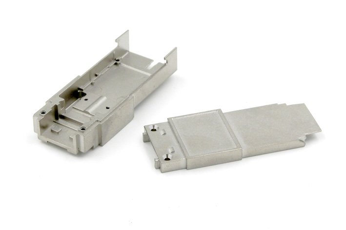
Stamping emerges as a pivotal manufacturing technique in the production of optical transceiver housings. This process involves the use of a press to shape or cut metal into desired forms. Stamping is renowned for its precision, which is essential for the intricate designs of optical transceiver housings. Additionally, the cost-effectiveness of stamping makes it an attractive choice for large-scale production. The scalability of the stamping process allows manufacturers to efficiently meet varying demands, from small batches to mass production.
Material Selection
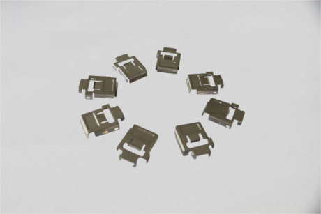
The materials commonly used for stamping the housing of optical transceivers are metals such as aluminum and stainless steel. These materials are favored due to their excellent conductivity, strength, and corrosion resistance. For example, aluminum provides a lightweight and sturdy option that is easy to use. Stainless steel provides excellent durability and lifespan. This is crucial for maintaining the integrity of the casing over time.
The stamping process for optical module housing generally comprises several key steps. The initial step, blanking, involves cutting the metal into flat pieces or blanks that will be further processed. This is followed by forming, where the blanks are shaped into the required three-dimensional configurations through bending, drawing, or other deformation techniques. The final step is finishing, which includes processes such as deburring, polishing, and coating to enhance the aesthetic and functional qualities of the housing. Each of these steps is crucial in achieving the high standards of quality necessary for optical transceiver housings, ensuring they meet the stringent requirements of telecommunications applications.
Benefits of Using Stamping for Optical Transceiver Housing
Stamping provides a very advantageous method for manufacturing optical transceiver housings, offering several significant benefits. One of the most important advantages is the ability to manufacture with high precision. Stamping allows the production of components with strict tolerances. Ensure that the optical module housing meets strict size and alignment requirements. This precision is crucial for maintaining the performance and reliability of optical modules, which are indispensable in telecommunications and data transmission applications.
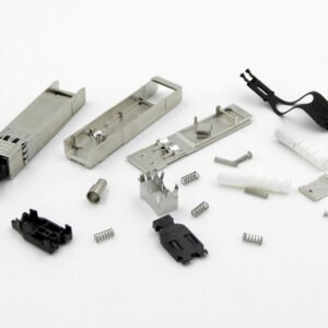
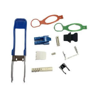
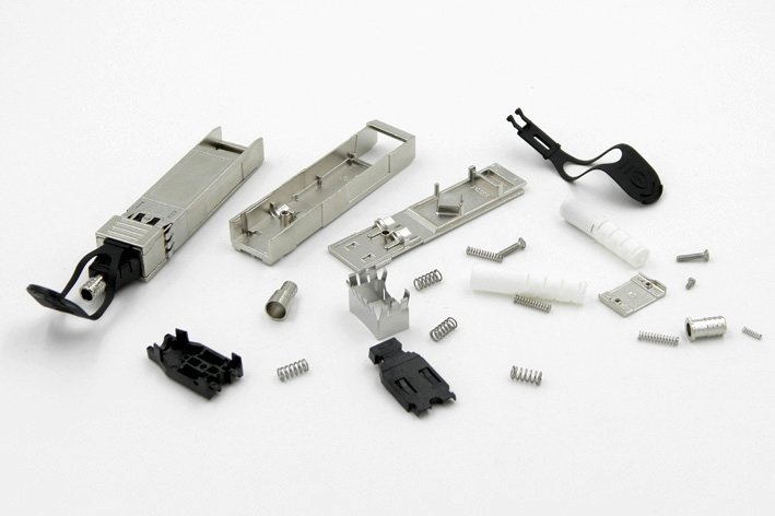
Another key benefit is the ability to generate complex shapes. Stamping technology is very suitable for creating complex geometric shapes. These geometric shapes may be difficult or costly to achieve through other manufacturing methods such as machining or casting. The flexibility of stamping enables the design of optical module housings to integrate various functional features such as mounting brackets, heat dissipation structures, and connection interfaces together.
The potential for mass production is another major advantage. Stamping is inherently scalable, making it ideal for high-volume production runs. This scalability translates into significant economic benefits, including reduced material waste and lower production costs. Compared to machining or casting, stamping uses raw materials more efficiently, resulting in less scrap and better utilization of resources. Additionally, the speed of the stamping process allows for faster production cycles, further driving down costs and lead times.
Challenge
Despite these benefits, the stamping process does present certain challenges. Tool wear is a common issue, as the repetitive nature of the process can lead to the degradation of stamping dies over time. Precise control over the stamping process is also essential to ensure consistent quality, which can be demanding and require sophisticated equipment. Additionally, material limitations can arise, as not all materials are equally suited for stamping, potentially restricting the choice of materials for optical module housings.
However, advancements in technology are helping to mitigate these challenges. The use of high-precision stamping presses enhances the accuracy and repeatability of the process, prolonging tool life and reducing maintenance needs. Moreover, advanced simulation software for designing stamping dies allows for detailed analysis and optimization before actual production, minimizing trial-and-error and improving overall efficiency. These technological innovations continue to push the boundaries of what can be achieved with stamping, making it an increasingly viable option for producing high-quality optical transceiver housings.
We sincerely hope to cooperate with you to build our future together!